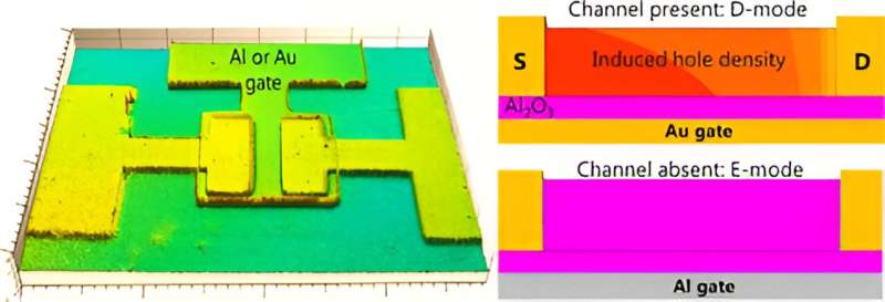
Graphical abstract. Credit: ACS Applied Electronic Materials (2024). DOI: 10.1021/acsaelm.3c01825
Nanoscale transistors are in demand for efficient digital circuits, and biasing of each device is critical. These stringent biasing conditions can be relaxed by obtaining precise values of the threshold voltages of the transistor. This leads to more tolerant logic states to the electrical noise.
To meet the requirements of reduced power consumption, CMOS field-effect transistors (FETs) are fabricated such that they operate in enhancement (E) mode, i.e., there are no free charge carriers in the channel at zero gate voltage. On the other hand, depletion (D) mode transistors have higher currents than enhancement mode due to ample charge carrier density.
In contrast to switching applications of FET, for high-frequency applications, off-state of FET is not a compulsory requirement. In fact, the presence of a channel at zero gate bias is advantageous to obtain high transconductance at lower voltages. For Si FETs, the enhancement or depletion modes were determined at the fabrication step of ion implantation doping. However, it is challenging to implement this solution for the new generation of thin materials like organic semiconductors and 2D materials.
According to new research published in ACS Applied Electronic Materials, by choosing a particular work function for a gate metal, threshold voltages of the p-type FETs can be changed from negative to positive values, which is selective switching between the enhancement mode and depletion mode of operation.
The researchers experimentally fabricated the FETs with various gate metal electrodes having different work functions. The dielectric alumina thickness was just 5 nm. Due to this short separation between the gate metal and organic p-type semiconducting channel, there was electrostatic interaction between them even without the application of external voltage. When low-work function metal like aluminum (4.4 eV) is used, the FET operates in enhancement mode.
For high-work function gate metals like gold (5.0 eV), a certain number of holes is induced in the channel at zero gate voltage. This leads to a good amount of current, which is known as depletion mode operation.
To confirm this experimental observation, the researchers performed TCAD device simulations. The simulations produced color contour plots of induced hole density. These kinds of matching experimental and simulation results are very important from the technological point of view and large-scale production.
The lead author, Dr. Abhay Sagade from SRMIST, India, revealed that the observed effects are profound for thin dielectric thicknesses such as those less than 10 nm. For larger thicknesses, the FETs remain in enhancement mode even for high-work function gate metals.
This concept can be easily extendable to any thin organic, inorganic, and new-generation 2D materials. Using this method, it should be possible to fabricate more compact-sized, accurate, and reconfigurable digital logic and oscillator devices and circuits. Further, D-mode OFETs with improved currents can be utilized efficiently for high-frequency applications.
This also has immense implications for upcoming quantum devices and technological applications that use small dimensional sensitive devices.
More information: Abhay A. Sagade, Selective Operation of Enhancement and Depletion Modes of Nanoscale Field-Effect Transistors, ACS Applied Electronic Materials (2024). DOI: 10.1021/acsaelm.3c01825
Provided by SRM Institute of Science and Technology


